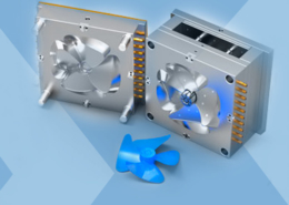
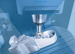
INJECTION MOULDING
Injection moulding parts and injection tools. Full solutions from design to production.
Investing in the UK’s injection moulding sector: The case for all-electric
Author:gly Date: 2024-09-30
Researchers at the National Institute of Advanced Industrial Science and Technology (AIST), have developed a microelectromechanical systems (MEMS) device fabrication technology that uses only printing and injection molding. This has been achieved by integrating the microfabrication technology and the MEMS design evaluation technology of AIST. A lighting device has been fabricated by combining the signal processing technology of Design Tech Co., Ltd. with the developed technology.
The injection-molding system used is commonly available in Japan. Injection-molding systems have lower market prices than semiconductor manufacturing systems and they have relatively low investment barriers. Japan is strong in the technologies for both mold-making and molding. Use of the developed technology is expected to enable non-semiconductor industries such as the plastics molding industry to begin manufacturing MEMS devices, which are products of only the semiconductor manufacturing sector so far. Entry of companies from different sectors into the MEMS manufacturing business will lead to the development of new applications of MEMS devices.
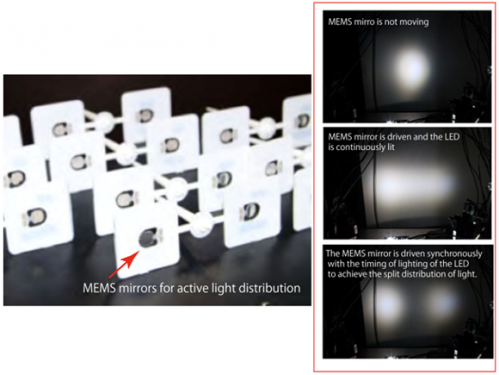
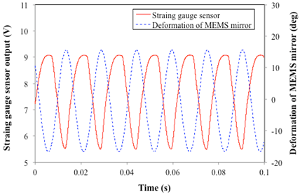
Figure 3 shows the displacement of the MEMS mirror for lighting and the output signal from the displacement sensor at different mirror angles. The displacement was directly measured with an optical measurement system. The resistance of the conductive ink changed in response to the displacement of the mirror, indicating that the displacement sensor worked properly.
With an expanding network of 25 locations throughout Australia and New Zealand, MM Plastics is steadfastly establishing the robust framework required to sustain its ongoing journey of expansion and growth.
The researchers have developed a technology for fabricating MEMS devices by using only printing and injection-molding processes. To do this, they have integrated fabrication and evaluation techniques obtained through the development of MEMS devices using semiconductor manufacturing processes and micro-molding technology that is low-cost and can be applied to mass production. This has led to the development of a MEMS device fabrication technology that requires reduced capital investment, can be applied to small-lot production, and has low production costs.
With over four decades of expertise, MPP has consistently provided top-tier components, products, and assemblies to a broad spectrum of industries, including Automotive, Consumer Goods, Safety, Spa & Pool, Building & Construction, Pharmaceuticals, Housewares, and more.
Get weekly and/or daily updates delivered to your inbox. You can unsubscribe at any time and we'll never share your details to third parties.
To develop applications of the developed MEMS device fabrication technology, the researchers intend to work actively with companies in a variety of industries and help to create opportunities for them to start new businesses.
Manufacturers’ Monthly is a business-to-business magazine and a valuable reference tool for all members of the manufacturing industry. The magazine is highly targeted and is read by key decision-makers who purchase and specify manufacturing equipment and services. It is also widely read by suppliers to the manufacturing industry.
Your email address is used only to let the recipient know who sent the email. Neither your address nor the recipient's address will be used for any other purpose. The information you enter will appear in your e-mail message and is not retained by Phys.org in any form.
Currently, the MM Plastics family is comprised of Dotmar Engineering Plastics, Graphic Art Mart, Fluoro Pacific, and Amari Visual Solutions.
Figure 1 shows the MEMS fabrication processes using printing and injection molding. First, a film for transfer of the MEMS functional layer is formed (Fig. 1b). The release layer and the MEMS functional layer are printed onto the film by using a screen or gravure printer. After alignment, the printed film is put into an injection mold (Fig. 1a and 1c). After the mold is closed, a molten resin is injected into it. The resin is then cooled and solidified into the MEMS structure (Fig. 1d). In the last step, the mold is opened and the MEMS structure is separated from the film removed from the mold. The ink layers printed on the film are thus transferred to the MEMS structure (Fig. 1e and 1f).
MM Plastics announces its acquisition of Micro Precision Plastics (MPP), a venerable family-owned leader in Injection Moulding and Manufacturing.
Premium Ad 7 $119,000 2019 JCB 531-70 AGRI FARM SPECIAL » Listing Type: Demo» Class: Agricultural Spec Location marker The shape of a location marker Ballarat, VIC 03 8373 7478 MESSAGE MORE DETAILS Premium Ad 15 $99,000 2005 JCB 531-70S 531-70 Agri super » Listing Type: Used» Class: General Spec Location marker The shape of a location marker Temora, NSW 02 8279 7084 MESSAGE MORE DETAILS Premium Ad 7 $65,450 2005 DIECI DEDALUS 28.7 » Listing Type: Used» Class: General Spec Location marker The shape of a location marker Donald, VIC 03 9998 4661 MESSAGE MORE DETAILS Premium Ad 4 $1,397 2023 ALLTRADES TRAILERS ALL-LOAD 1.5TON ALR/1.5-2.4 » Listing Type: Used Location marker The shape of a location marker Yatala, QLD 1300794266 MESSAGE MORE DETAILS Premium Ad 4 $1,265 2023 ALLTRADES TRAILERS ALL-LOAD 1.5TON ALR/1.5-2.0 » Listing Type: New Location marker The shape of a location marker Yatala, QLD 1300794266 MESSAGE MORE DETAILS Premium Ad 5 $13,200 POA (HIRE) PRENTICE 7,000KG SWL » Listing Type: Used Location marker The shape of a location marker Granville, NSW 1800 688 788 MESSAGE MORE DETAILS Premium Ad 19 $28,000 2007 MANITOU MT1435SL » Listing Type: Used» Class: Construction Spec» Operating weight - kg: 10,000 Location marker The shape of a location marker Mooloolaba, QLD 07 3073 8194 MESSAGE MORE DETAILS Premium Ad 9 $13,000 20FT CONTAINER SIDE OPENING » Listing Type: New Location marker The shape of a location marker Shepparton North, VIC 03 8373 7109 MESSAGE MORE DETAILS Premium Ad 4 $3,750 YALE MP15UX » Listing Type: New Location marker The shape of a location marker Griffith, NSW 02 6171 3171 MESSAGE MORE DETAILS Premium Ad 91 $80,800 2013 CATERPILLAR TH514 with Hydraulic Quick Hitch » Listing Type: Used» Class: Construction Spec» Lift capacity at maximum height - kg: 2,000» Maximum lift height - mm: 13,700» Operating weight - kg: 11,340 Location marker The shape of a location marker Singleton, NSW 02 8315 0202 MESSAGE MORE DETAILS Premium Ad 9 $125,000 2016 JCB 541-70 S » Listing Type: Used» Class: General Spec Location marker The shape of a location marker Ballarat, VIC 03 8373 7478 MESSAGE MORE DETAILS Premium Ad 3 $42,900 1992 JCB LOADALL 525-58 » Listing Type: Used» Class: General Spec Location marker The shape of a location marker Donald, VIC 03 9998 4661 MESSAGE MORE DETAILS
Use this form if you have come across a typo, inaccuracy or would like to send an edit request for the content on this page. For general inquiries, please use our contact form. For general feedback, use the public comments section below (please adhere to guidelines).
Figure 2 shows examples of MEMS devices fabricated by using the developed technology. A reflective mirror and a mirror displacement sensor are incorporated into the MEMS mirror device for lighting (Fig. 2a). A mirror ink for the reflective mirror, a conductive ink for the strain sensor, and a magnetic ink for driving the mirror are printed on the film, and then the printed ink patterns are transferred to the MEMS structure by injection molding. The MEMS mirror device for lighting did not break after more than 100 million operations driven by an external coil. A MEMS device array can be fabricated using an arrayed MEMS pattern mold (Fig. 2b).
The MEMS device fabrication technology using printing and injection molding enables the low-cost fabrication of various MEMS devices, for example sensing devices such as acceleration sensors and gas sensors, and power generation devices, by changing the printed MEMS functional layers in accordance with the purpose. This makes it possible to provide low-cost MEMS devices in fields where MEMS devices cannot currently be used owing to the high cost of MEMS fabricated using conventional semiconductor manufacturing processes. For example, in the lighting industry, light distribution control of LED lighting is attracting attention. When MEMS mirrors are produced using semiconductor manufacturing processes, the production cost depends on the number of devices per wafer. Therefore, the production cost of large mirrors is very high, while the use of micro-mirrors requires convergence of light, making the lens optical system complex. The developed technology can be used to produce low-cost large MEMS devices (larger than several millimeters across) and therefore active light distribution control devices can be realized easily.
The developed technology makes it possible to fabricate MEMS devices by using the printing technology that enables the fabrication of large-area devices without a vacuum process and the injection-molding technology that requires small capital investment and enables low production costs. MEMS devices currently produced by using semiconductor manufacturing processes can now be fabricated inexpensively and with a small capital investment. This allows the applications of MEMS devices in fields where MEMS cannot currently be used owing to high production costs and low production volumes. For example, new applications in the lighting industry can be developed by combining active variable light distribution by a MEMS mirror and LED lighting.
MM Plastics, a distinguished name in the Australian plastics industry, now further solidifies its presence with the addition of Micro Precision Plastics.
MEMS devices fabricated by using this technology will be presented at the Micromachine/MEMS Exhibition held at Tokyo Big Sight (Koto-ku, Tokyo) from July 11 to 13, 2012 and at AIST Open Lab held at AIST Tsukuba from October 25 to 26, 2012.
To drive a MEMS device, patterns of wiring and functional materials need to be formed onto moving microstructures. Attempts have been made to use resins for MEMS structures. However, the production cost is high because the same vacuum processes as that used in semiconductor manufacturing are used to form the metal wiring pattern. The researchers have realized the low-cost fabrication of resin MEMS structures in which the patterns of metal wiring and functional materials are formed using a low-cost printing process and transferred to the structure using an injection-molding process. Moving MEMS structures, such as springs and cantilevers, must be thin. However, it has been difficult to form thin resin structures because a molten resin begins to harden immediately after being injected into the mold. The researchers have made it possible to fill thin moving structures with a resin by improving the mold structure. Thus MEMS devices can be fabricated by using a molding process. This fabrication technique can be used to form MEMS structures inexpensively by using only a replica molding technique once the mold is created.
This R&D project was supported by the Funding Program for World-leading Innovative R&D in Science and Technology, "Research and Development of Integrated Microsystems", of the Japanese Cabinet Office.
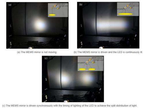
Figure 4 shows examples of the distribution of light to left and right by controlling the drive of the MEMS mirror synchronously with the timing of lighting of the LED. Active light distribution was achieved with the MEMS mirror. Figure 5 is the light distribution characteristics. The light distribution was changed between spread angles of 10° (Fig. 4a and the red line in Fig. 5) and 50° (Fig. 4b and the blue line in Fig. 5) by controlling the drive of the MEMS mirror. As shown in Fig. 4c and by the green line in Fig. 5, the light can be split by controlling the drive of the MEMS mirror synchronously with the timing of lighting of the LED. In the next step, the researchers will improve the symmetry and expand the range of the light distribution by improving the arrangement of the optical system, the signal processing, and the control circuit. Injection molding can be used easily to form three-dimensional objects of complex shape such as spheres, and the researchers expect MEMS devices to be formed on the surface of, or inside, three-dimensional objects.
Nestled in the heart of Dandenong South, Victoria, MPP boasts a remarkable operation featuring 22 cutting-edge injection moulding machines.
This state-of-the-art facility is dedicated to crafting high-quality components that meet rigorous global standards. Going beyond manufacturing, MPP offers a comprehensive suite of value-added services, encompassing toolmaking, engineering, material selection, and product assembly.
AIST has a test mass-production line for 8-inch-wafer MEMS and has been working on the test mass-production and development of MEMS devices in collaboration with the private sector. The present researchers are also developing a micro-molding technology that uses nanoimprinting and injection molding. They have developed large-area nanostructured anti-reflective lenses and substrates with controlled hydrophilicity/hydrophobicity that utilize nanostructures.
Mousa Elsarky, Executive General Manager of MM Plastics, expressed his enthusiasm for this strategic move saying, “We are very excited to welcome Micro Precision Plastics into the MM Plastics family. We are constantly seeking exceptional opportunities to expand our business to better serve the Australian and New Zealand markets across various plastic segments.”
We keep our content available to everyone. Consider supporting Science X's mission by getting a premium account.
MEMS devices such as acceleration sensors, gyro sensors, and mirror devices for displays are currently commercially available. However, conventional MEMS fabrication techniques use the same semiconductor manufacturing systems that are used to produce large- and small-scale integrated circuits, and they require several tens of processes, including vacuum processes. MEMS fabrication therefore requires large capital investment and has high production costs that cause problems.
LK-Mould Ltd.,
No.15, JinShen Road, Jin xia District
Changan Town, Dongguan
523850 Guangdong
China